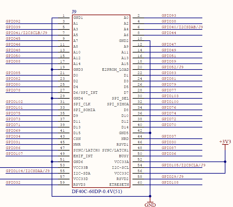
J9 Pin Configuration (Design Error)
Delfino Datasheet
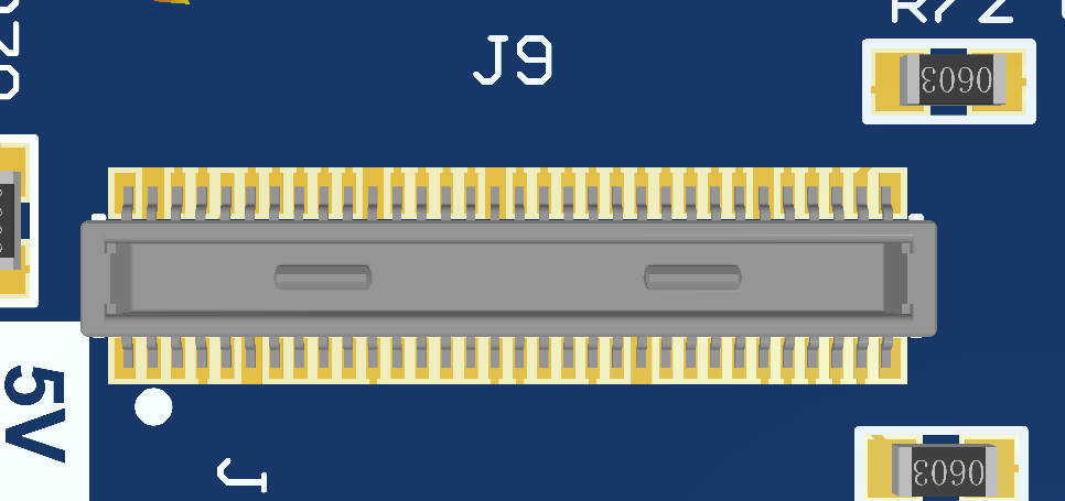
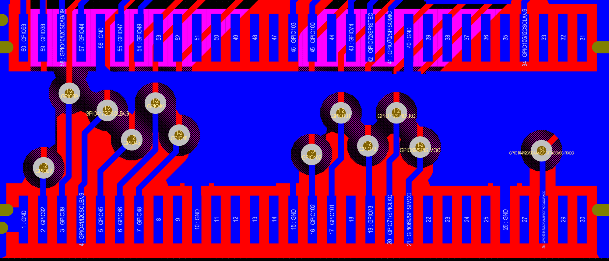
Altium PCB
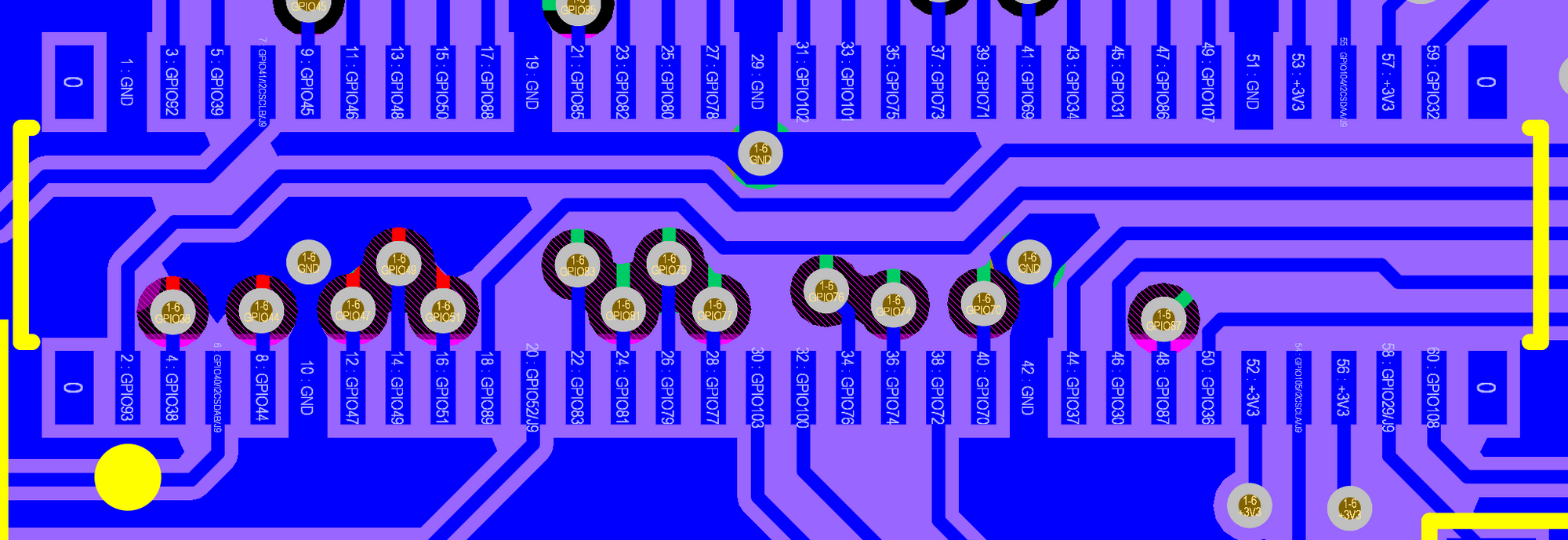
Delfino PCB
J9 Adapter PCB
Adaptor PCB
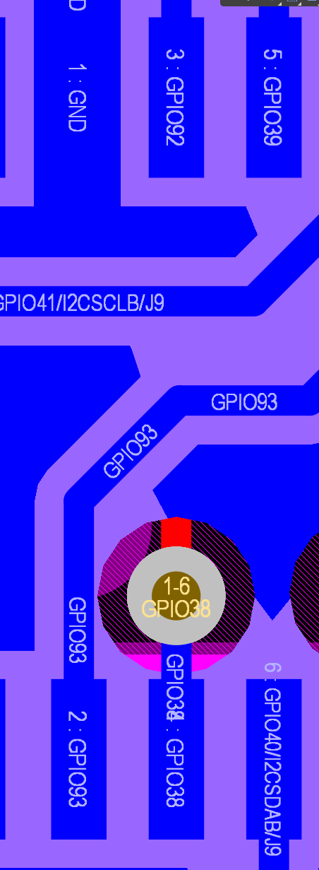
The schematic symbol pin configuration doesn't match up with the footprint symbol
The design follows the schematic pin configuration. Hence some connections will be assign to GND or 3.3V resulting it unusable
Usuable Pins
(16 + 2) out of 24pins are useable
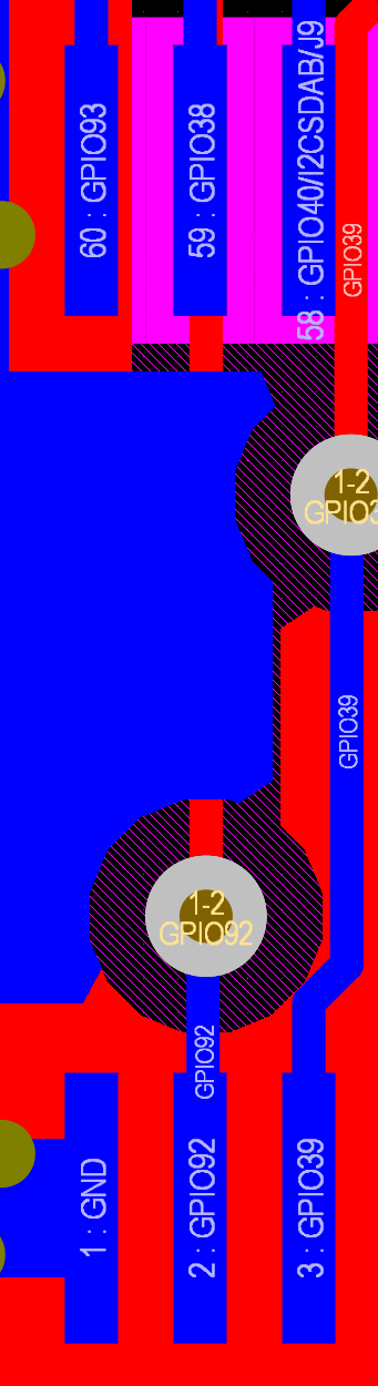
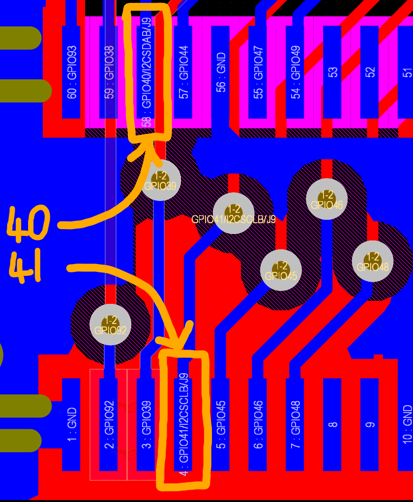
2 is GPIO40 & GPIO41
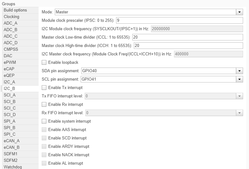
GPIO40 and GPIO41 Investigation
Continuity test prove that the pins are connected.
Pins are separated - Cant be shorted together, other pins works
Datasheet state that the port is capable of Input / Output
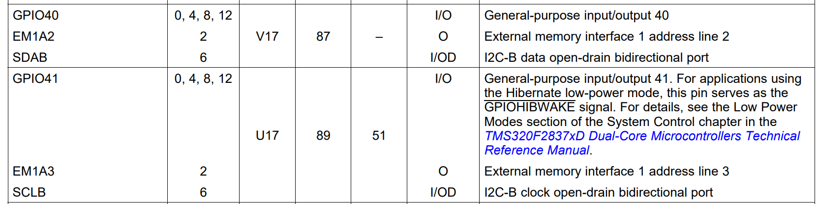
Cant be disable, changing the SDA and SCL pin assignment doesn't help