


Running Code From RAM
Simulink → C File (biss_pure_spi_32bits_v2)
Simulink Coder Custom Code Block
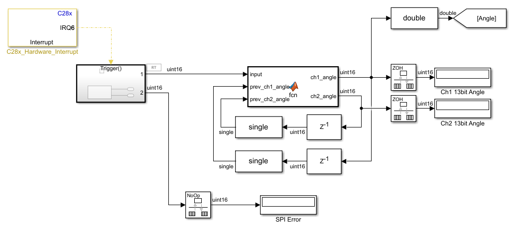
biss_fpga_spi_interrupt.slx
Simulink Block Diagram
Interrupt File - MW_c28xx_csl.c - SPIB_RX_INT_isr
interrupt void SPIB_RX_INT_isr(void)
{
isr_int6pie3_task_fcn();
EALLOW;
SpibRegs.SPIFFRX.bit.RXFFINTCLR = 1;
EDIS;
PieCtrlRegs.PIEACK.all = PIEACK_GROUP6;
/* Acknowledge to receive more interrupts*/
}
C++
biss_fpga_spi_interrupt_data.c - isr_int6pie3_task_fcn
/* Hardware Interrupt Block: '<Root>/C28x_Hardware_Interrupt' */
void isr_int6pie3_task_fcn(void)
{
if (1 == runModel) {
/* Call the system: <Root>/Subsystem */
{
/* S-Function (c28xisr_c2000): '<Root>/C28x_Hardware_Interrupt' */
/* Output and update for function-call system: '<Root>/Subsystem' */
{
MW_SPI_FirstBitTransfer_Type MsbFirstTransferLoc;
MW_SPI_Mode_type ClockModeValue;
uint16_T rdDataRaw;
uint16_T status;
/* MATLABSystem: '<S3>/SPI Receive' */
if (biss_fpga_spi_interrupt_DWork.obj.SampleTime !=
biss_fpga_spi_interrupt_P.SPIReceive_SampleTime) {
biss_fpga_spi_interrupt_DWork.obj.SampleTime =
biss_fpga_spi_interrupt_P.SPIReceive_SampleTime;
}
ClockModeValue = MW_SPI_MODE_0;
MsbFirstTransferLoc = MW_SPI_MOST_SIGNIFICANT_BIT_FIRST;
status = MW_SPI_SetFormat
(biss_fpga_spi_interrupt_DWork.obj.MW_SPI_HANDLE, 16U, ClockModeValue,
MsbFirstTransferLoc);
if (status == 0U) {
MW_SPI_Read_16bits(biss_fpga_spi_interrupt_DWork.obj.MW_SPI_HANDLE,
&rdDataRaw, 1UL, 0U);
}
/* MATLABSystem: '<S3>/SPI Receive' */
biss_fpga_spi_interrupt_B.SPIReceive_o1 = rdDataRaw;
}
/* End of Outputs for S-Function (c28xisr_c2000): '<Root>/C28x_Hardware_Interrupt' */
}
}
}
C++
MW_SPI
C:\ProgramData\MATLAB\SupportPackages\R2021b\toolbox\target\supportpackages\tic2000\inc\MW_c2000SPI.h
/* Initiate SPI data read */
inline Uint16 MW_SPI_Read_16bits(MW_Handle_Type SPIModuleHandle, Uint16 * rdData, Uint32 datalength, Uint16 blockingMode)
{
#ifndef MATLAB_MEX_FILE
MW_SpiHandle mySpi = (MW_SpiHandle)SPIModuleHandle;
volatile struct SPI_REGS *SPI = (struct SPI_REGS *)mySpi->spi_base_address;
Uint32 localVar = 0;
Uint16 ret = 0;
Uint16 *readdata = (Uint16*) rdData;
if (blockingMode == 0)
{
ret |= (*SPI).SPIFFRX.bit.RXFFOVF;
for (localVar = 0; localVar < datalength; localVar++)
{
if ((*SPI).SPIFFRX.bit.RXFFST > 0)
{
readdata[localVar] = (*SPI).SPIRXBUF & (((Uint32)1 << mySpi->charLength) - 1);
}
else
{
ret |= 0x02;
}
}
}
else
{
for (localVar = 0; localVar < datalength; localVar++)
{
while ((*SPI).SPIFFRX.bit.RXFFST == 0)
{
/*Wait until Rx buffer has data*/
}
readdata[localVar] = (*SPI).SPIRXBUF & (((Uint32)1 << mySpi->charLength) - 1);
}
}
return ret;
#else
return -1;
#endif
}
C++
MW_SPI_MasterWriteRead_8bits
/* Initiate combined SPI transmission from master to slave */
MW_SPI_Status_Type MW_SPI_MasterWriteRead_8bits(MW_Handle_Type SPIModuleHandle, const uint8_T * wrData, uint8_T * rdData, uint32_T datalength)
{
#ifndef MATLAB_MEX_FILE
MW_SpiHandle mySpi = (MW_SpiHandle)SPIModuleHandle;
volatile struct SPI_REGS *SPI = (struct SPI_REGS *)mySpi->spi_base_address;
uint32_T localVar;
uint16_T *readdata = (uint16_T*) rdData;
uint16_T *writedata = (uint16_T*) wrData;
for (localVar = 0; localVar < datalength; localVar++)
{
while ((*SPI).SPIFFTX.bit.TXFFST == mySpi->fifoLevel)
{
/*Wait until Tx buffer is cleared*/
}
(*SPI).SPITXBUF = writedata[localVar] << (16 - mySpi->charLength);
while ((*SPI).SPIFFRX.bit.RXFFST == 0)
{
/*Wait until Rx buffer has data*/
}
readdata[localVar] = (*SPI).SPIRXBUF & (((Uint32)1 << mySpi->charLength) - 1);
}
return MW_SPI_SUCCESS;
#else
return MW_SPI_SUCCESS;
#endif //MATLAB_MEX_FILE
}
C
MW_SPI_Write_16bits
/* Initiate SPI data write */
inline Uint16 MW_SPI_Write_16bits(MW_Handle_Type SPIModuleHandle, const Uint16 * wrData, Uint32 datalength, Uint16 blockingMode)
{
#ifndef MATLAB_MEX_FILE
MW_SpiHandle mySpi = (MW_SpiHandle)SPIModuleHandle;
volatile struct SPI_REGS *SPI = (struct SPI_REGS *)mySpi->spi_base_address;
Uint32 localVar;
Uint16 ret = 0;
Uint16 *writedata = (Uint16*) wrData;
if (blockingMode == 0)
{
for (localVar = 0; localVar < datalength; localVar++)
{
if ((*SPI).SPIFFTX.bit.TXFFST < mySpi->fifoLevel)
{
(*SPI).SPITXBUF = writedata[localVar] << (16 - mySpi->charLength);
}
else
{
ret = 1;
}
}
}
else
{
for (localVar = 0; localVar < datalength; localVar++)
{
while ((*SPI).SPIFFTX.bit.TXFFST == mySpi->fifoLevel)
{
/*Wait until Tx buffer is cleared*/
}
(*SPI).SPITXBUF = writedata[localVar] << (16 - mySpi->charLength);
}
}
(*SPI).SPIFFTX.bit.TXFFIENA = mySpi->txInterrupt; /* SPI Tx Interrupt mode*/
(*SPI).SPIFFTX.bit.TXFFINTCLR = 1; /* Clear Tx FIFO Interrupt flag*/
return ret;
#else
return -1;
#endif
}
C
Custom Code
Clear SPIB Buffer
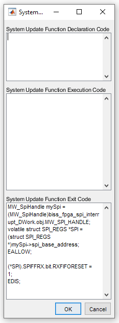
MW_SpiHandle mySpi = (MW_SpiHandle)biss_fpga_spi_interrupt_DWork.obj.MW_SPI_HANDLE;
volatile struct SPI_REGS *SPI = (struct SPI_REGS *)mySpi->spi_base_address;
(*SPI).SPIFFRX.bit.RXFIFORESET = 1;
C++
SPI Description (Technical Reference Manual pg2234)
Programmable interrupt levels.
Both transmit and receive FIFOs can generate CPU interrupts and
DMA triggers. The transmit interrupt (SPITXINT) is generated whenever the transmit FIFO status bits
(TXFFST) match (less than or equal to) the interrupt trigger level bits (TXFFIL). The receive interrupt
(SPIRXINT) is generated whenever the receive FIFO status bits (RXFFST) match (greater than or
equal to) the interrupt trigger level RXFFIL. This provides a programmable interrupt trigger for transmit and receive sections of the SPI. The default value for these trigger level bits will be 0x11111 for receive FIFO and 0x00000 for transmit FIFO, respectively.
TXFFST ≤ TXFFIL → Interrupt
RXFFST ≥ RXFFIL → Interrupt
EALLOW (Bit 6) — Emulation access enable bit.
This bit, when set, enables access to emulation and other protected registers. Set this bit by using
the EALLOW instruction and clear this bit by using the EDIS instruction. See the data sheet for a
particular device to determine the registers that are protected.
When the CPU services an interrupt, the current value of EALLOW is saved on the stack (when
ST1 is saved on the stack), and then EALLOW is cleared. Therefore, at the start of an interrupt
service routine (ISR), access to protected registers is disabled. If the ISR must access protected
registers, it must include an EALLOW instruction. At the end of the ISR, EALLOW can be restored
by the IRET instruction.
EDIS
Disable access to emulation space and other protected registers.
This instruction clears the EALLOW bit in status register ST1. When this bit is clear, the
C28x CPU does not allow write access to the memory−mapped emulation registers and
other protected registers. See the data sheet for your particular device to determine
which registers the EALLOW bit protects.
To allow write access to the registers, use the EALLOW instruction.