
Power Source
+5V
Delfino (Powered from MiniUSB)
FPGA (Powered from MicroUSB)
External

Only one source could be connected to 5V at any one time. Connecting multiple +5V could damage the components
Short J1 to use 5V from FPGA (If FPGA is powered from MicroUSB)
or
Short J1 to power the FPGA from other 5V source
Short J3 to use 5V from Delfino
Signal
Delfino
I/O Voltage: 3.3V
FPGA
I/O Voltage: 3.3V
BiSS Encoder
I/O Voltage: 5V
Transceiver (Datasheet)
High-level input voltage (driver, driver enable, and receiver enable inputs)
Min 2V
Typical: 3.3V
Max Vcc
Low-level input voltage (driver, driver enable, and receiver enable inputs)
Min 0V
Typical: 0V
Max 0.8V
FPGA Bypass
The board could feed BiSS signal directly from CH1 transceiver to the SPI Bus
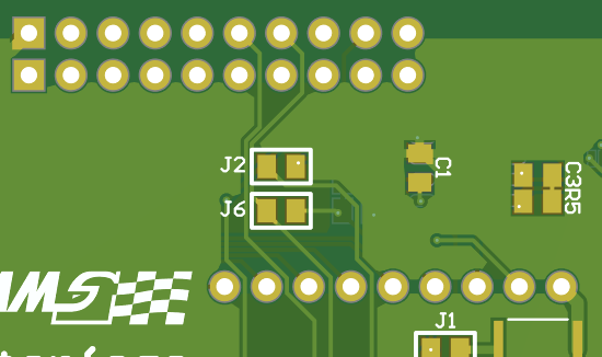
Short J2 and J6 to bypass FPGA (FPGA shouldn't be installed when bypassed)
CH2 can't be bypass
Voltage Divider Value
Voltage divider circuit is only required for FPGA use
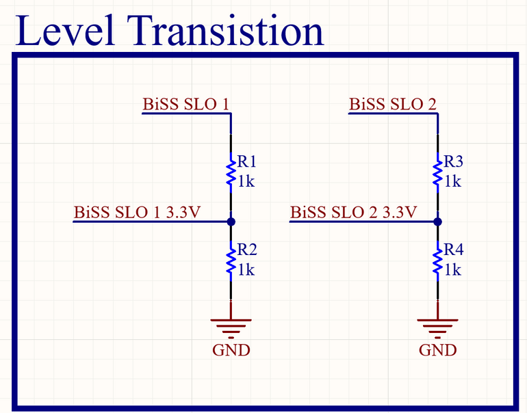
The value in the schematic doesn't reflect the latest resistor value used.
According to this test Testing: Using Voltage Divider
The recommended value is:
Software (Non-FPGA)
Simulink Files (Last Update: 1-Jul-21)
Setup
SPI
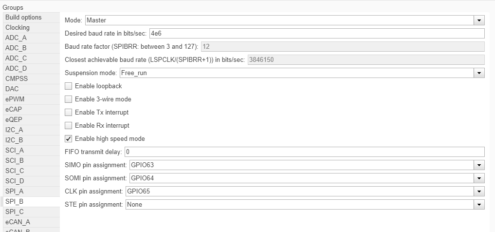
SPI_B frequency is 4MHz
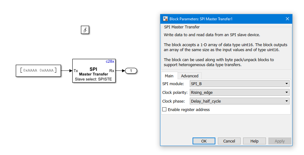
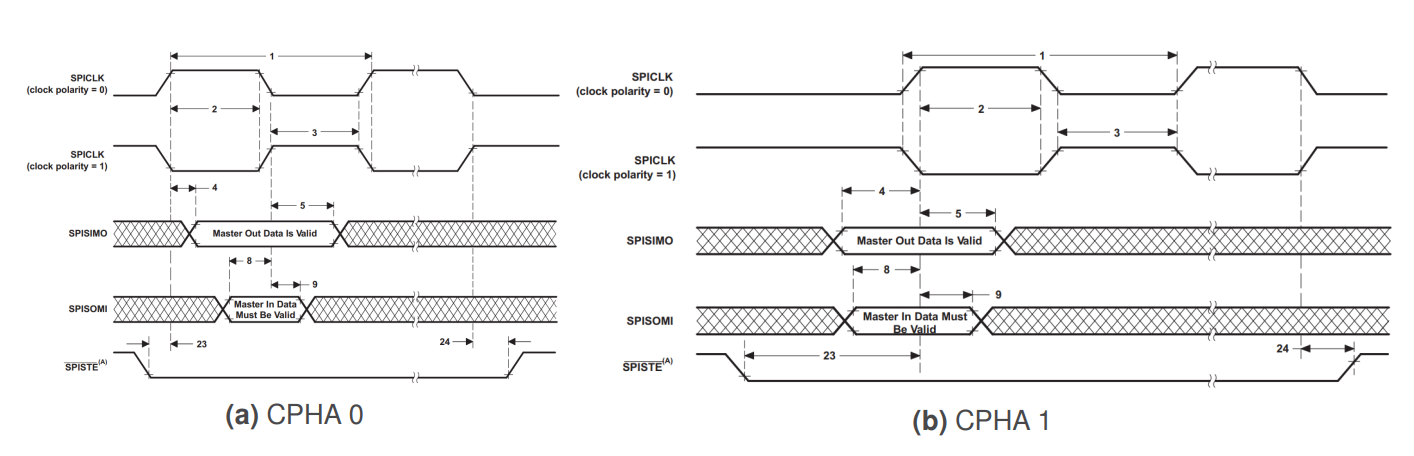
In hardware SPI handler → subsystem. Clock polarity is always "Rising Edge Falling Edge"
Clock Phase: (Reference this figure)
Delay_half_cycle → When using <1MHz (Sample at falling clock edge)
No_delay → When using 4MHz (Sample at rising clock edge)
Integration
The program is modular, All BiSS related process is implemented in the subsystem.
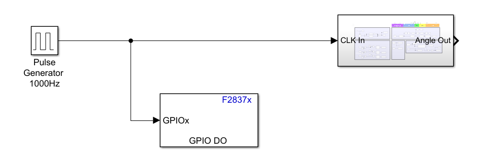
BiSS is sampling at 1kHz
Each rising edge from the pulse generator will trigger BiSS to sample
Angle will be available at Angle Out in 13bits (0 to 8191) form
Comment out "Error Counter" if there is SCI bandwidth issue
Comment out all Display when not debugging